Problem
Board geometry
Fix
- Verified fitment using SolidWorks and 3D printing
- Picked small components that can still be hand-soldered
- Optimized traces so the power plane is not bottlenecked

Engineering portfolio Fayetteville, AR
Mechanical and Electrical
Procedural board, routed live in your browser — not one of my layouts. Readouts follow your cursor.
Scope
I design the circuit board — and the bracket it bolts to.
Two degrees, one bench. Schematic to layout, CAD model to machined part.
Arkansas Space Grant Consortium
Electrical Engineering Senior Design
I led the electrical team. We built one custom board to power the Jetson Nano, run the motor and servo, and read an accelerometer — as small and as cheap as we could make it.
Objective
Develop a custom PCB to efficiently power and manage communication for a Jetson Nano, motor, and servo control system — while integrating accelerometer data, minimizing board size, and reducing overall project cost.
My job as ELEG team leader

Signature · 3D
My board, rebuilt in 3D from the layout — fabricated, populated, then powered up.
3D reconstruction from the layout — illustrative
Twelve callouts from my layout. Copper is power; green is logic and I/O.

One board between the battery, the Jetson, and everything that moves. Hover or tap a block to trace its connections.
Packet motion is illustrative — not recorded data

Four sheets, drawn in Cadence. Hover a sheet to read it; click to open it full size.Swipe the sheets; tap one to open it full size.


Semester 1 · Fall 2024
Semester 2 · Spring 2025


Problem
Fix
Problem
Fix


Fig. 7 — Mod board
UnitELEG board
EventASGC Autonomous Vehicle Challenge
Summary6 / 6 pass
| # | Area | Result | Status |
|---|---|---|---|
| 01 | Deadline | PCB built and programmed by the March 1st deadline | PASS |
| 02 | Hardware | No fires or short circuits | PASS |
| 03 | Hardware | Board functioned throughout the whole competition | PASS |
| 04 | Competition | 2nd place finish | PASS |
| 05 | Competition | Motor and servo worked as instructed by the Jetson | PASS |
| 06 | Competition | The car started every lap | PASS |
Antenna Design Coursework
Individual RF project. I designed a probe-fed T-patch in Ansys HFSS, generated the Gerbers in KiCad, machined it, and put it on a VNA. The hardware didn’t match the simulation — both results are below.
Objective Develop a patch antenna in Ansys and compare the simulated results to the manufactured antenna.
| Parameter | Value | Note |
|---|---|---|
| Geometry | T-shaped patch | |
| Center freq. | 2.4 GHz | |
| S11 | −12.84 dB | at 2.4 GHz, simulated |
| Size | < 13 × 13 cm | constraint |
| Connector | SMA, 50 Ω | |
| Feed | Probe-fed | with ground plane |
Scroll to sweep · drag the marker Use the softkeys to step the marker
Dashed box: the 13 cm × 13 cm size constraint. Green rings mark the SMA probe feed.
Undersize drawn for clarity — the actual amount wasn’t measured
Sliding dip: illustration of the shift — not recorded data
Sim trace: approximation traced from the HFSS plot (2–3 GHz)
Ansys HFSS. I tuned patch length, width and the SMA feed’s x/y position to land resonance at 2.4 GHz.
A problem with the endmill left the patch smaller than the simulated dimensions.
Keysight N9914B. Smaller patch, higher resonance: −2.7 dB near 2.7 GHz.
| Mkr | Freq (GHz) | S11 (dB) |
|---|---|---|
| M1 | 1.9958328 | −2.440 |
| M2 | 2.6773623 | −2.765 |
| M3 | 3.8087422 | −3.834 |
KiCad Gerbers, then machined. This is the board that went on the VNA.

The machined antenna did not match simulation: a problem with the endmill left the patch smaller than the simulated dimensions, which pushed resonance up — the measured response sits at −2.7 dB near 2.7 GHz. In simulation, patch length and width and the x/y position of the SMA feed were the variables tuned to land the resonant frequency.
HFSS also solved the far field. The orbitable lobe here is a sketch of that shape over the ground plane and the T-patch. The gain plot is the actual simulation output.
Illustrative pattern shape — see the HFSS gain plot
Push Plastic · Engineering Intern
Objective Design a solution that uses Keyence lasers to measure and record 3D-printing filament diameter.
Laser micrometers, an Arduino Nano, a Python logger, and printed mounts on a pole that moves to whichever production line needs it.
Keyence laser micrometers read the filament diameter as the strand passes through.
An Arduino Nano talks to the lasers and hands the readings to the PC over USB.
My Python 3.11 program starts and stops recording, saves to .csv, and plots the live value.
Later, it was set up to stop the winding if product was recorded out of spec.
Animated illustration: filament leaves the extruder, passes two laser micrometer heads mounted on a pole with the display, and winds onto a spool. Pressing Inject defect sends an oversize section down the line; when it is measured out of spec the winder stops until the fault is acknowledged.
Illustration of the system's logic — not recorded production data
Diameter deviation exaggerated for visibility
mm
RECrows → data_log.csv 000000
Line running — in spec
Recorded out of spec stop winding
Three layers. Each one had to work before the next one had anything to say.
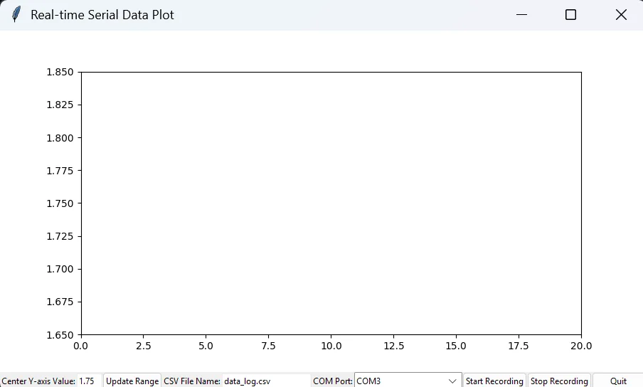
Designed in Fusion 360, sliced in Prusa and Bambu slicers, printed, and mounted to the pole.
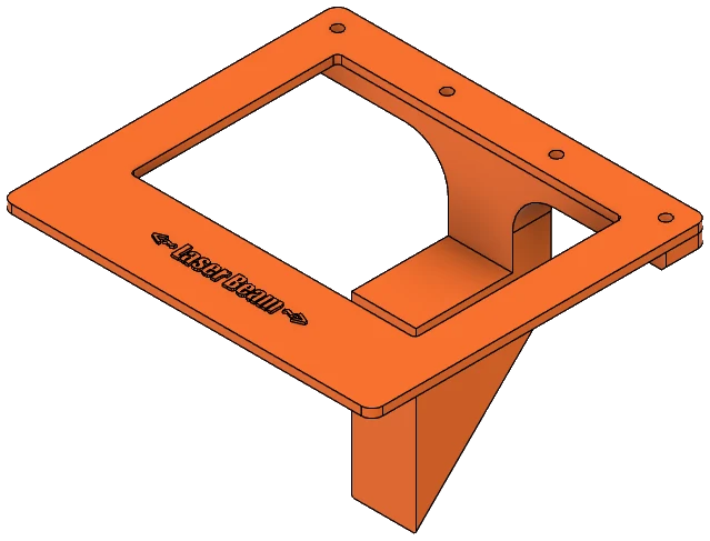
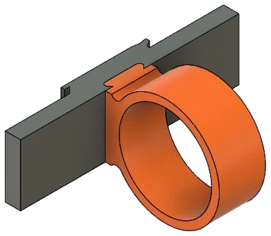

Movable pole Every component mounts to one movable pole, so the system can be used on every production line.
Communication with the lasers.
I contacted support and got help from coworkers.
The system worked as expected: the Arduino relayed data from the lasers to a computer running the Python program. It was later set up to stop the winding process if product was recorded out of specification.
↑ That last part is the halt the line above simulates.
University of Arkansas · Research Assistant
Objective Design a small PCB for a research grant: amplify a signal, reduce the size as much as possible, and integrate a display and user buttons.
Challenge · PCB size
The board had to stay small. To keep it at 1.5 in × 1.5 in, I moved it from a 2-layer board to a 4-layer board.
Layer artwork is illustrative; top layer is the real board

PCB size
Moved from a 2-layer board to a 4-layer board.
Communication
Set up meetings and kept a project notebook for reference and record.
Drawn in Cadence. Open it to pan and zoom.
Completed under the guidance of an advisor. I was responsible for the schematic, the layout design, and the bill of materials. After fabrication, the power section of the board was functional by the start of the fall semester.
Experience · Leadership · Skills
I started as a mechanic: 40 hours a week while carrying 8–10 credits a semester. Then five internships in four summers, across both degrees.
Mechanic → Shift Lead Mechanic
Internship
Ammonia System Design Engineer (internship)
Internship
Research Assistant (internship)
Internship
University of Arkansas · May 2026
3 channels · 2022 – 2024
Institute of Electrical and Electronics Engineers
President / Treasurer
2023 – 2024
Amateur Radio Club at the University of Arkansas
Treasurer
2022 – 2024
American Indian Science and Engineering Society
Treasurer
2022 – 2023
Off the clock
In progress
Building an actively stabilized rocket for a Level 1 certification.
Illustrative motif — not flight dataBuilt
Designed and manufactured a machine that climbs rope using stored mechanical energy.
Illustrative motif — not a recording19 line items · skills
| Ref | Part | Category | Qty |
|---|---|---|---|
| U1 | Cadence (schematic → PCB) | Electrical | 1 |
| U2 | PSpice (schematic → PCB layout) | Electrical | 1 |
| U3 | KiCad | Electrical | 1 |
| U4 | Ansys HFSS | Electrical | 1 |
| U5 | STM32CubeIDE | Electrical | 1 |
| U6 | Arduino | Electrical | 1 |
| U7 | Allen-Bradley PLC | Electrical | 1 |
| U8 | Delta HMI | Electrical | 1 |
| M1 | SolidWorks (incl. FEA) | Mechanical | 1 |
| M2 | Fusion 360 | Mechanical | 1 |
| M3 | Fusion 360 toolpath generation | Mechanical | 1 |
| M4 | CATIA drafting | Mechanical | 1 |
| M5 | Metal fabrication | Mechanical | 1 |
| M6 | CNC machining | Mechanical | 1 |
| M7 | 3D printing | Mechanical | 1 |
| S1 | Python 3.11 | Software | 1 |
| S2 | Arduino IDE | Software | 1 |
| S3 | STM32CubeIDE | Software | 1 |
| S4 | Monday (project management) | Software | 1 |
Close the circuit
BSME and BSEE, University of Arkansas, May 2026. Email is the best way to reach me.
Illustrative schematic — a metaphor, not a real circuit